ATmega32 Microcontroller Pin Diagram
For explaining the ATmega32 Microcontroller Pin diagram, consider a 40-pin Dual Inline Package (DIP) of microcontroller integrated circuit is:
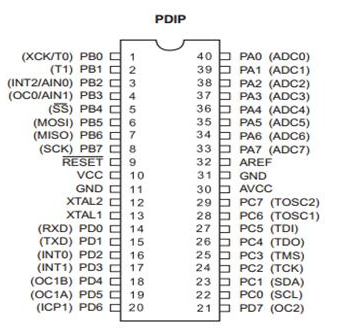
Pin Descriptions:
Port A (PA7-PA0): Port A serves as analog inputs for A/D converter. It also acts as an 8-bit bidirectional I/O port if the A/D converter is not used internally.
Port B (PB7-PB0) and Port D (PD7-PD0): These ports are 8-bit bidirectional I/O ports. Their output buffers have symmetrical drive characteristics with high source and sink capability. As inputs, these are pulled low if the pull-up resistors are used. It also provides various special functional features of the ATmega32.
Port C (PC7-PC0): Port C is an 8-bit bidirectional I/O port. If the Joint Test Action Group (JTAG) interface is enabled, the pull-up resistors on pins PC2 (TCK), PC3 (TMS), and PC5 (TDI) will be activated.
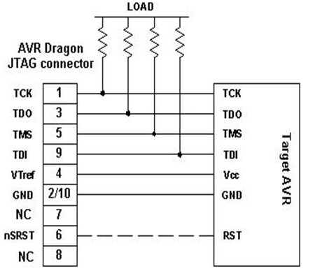
Consider the interfacing of Joint Test Action Group (JTAG) using Port C of ATmega32 is:-
Vcc: Digital voltage supply
GND: Ground
RESET: It is a RESET pin which is utilized to set the microcontroller ATmega32 to its primary value. During the beginning of an application the RESET pin is to be set elevated for two machine rotations.
XTAL1: It is an input for the inverting oscillator amplifier and input to an internal clock operating circuit.
XTAL2: It is an output from an inverting oscillator amplifier.
AVcc: It is a supply voltage pin for A/D converter and Port A. It must be connected with Vcc.
AREF: AREF is an analog signal reference pin for the analog to digital converter.