86
Binary Adder
The Add micro-operation requires registers that can hold the data and the digital components that can perform the arithmetic addition.
A Binary Adder is a digital circuit that performs the arithmetic sum of two binary numbers provided with any length.
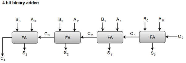
A Binary Adder is constructed using full-adder circuits connected in series, with the output carry from one full-adder connected to the input carry of the next full-adder.
The following block diagram shows the interconnections of four full-adder circuits to provide a 4-bit binary adder.

- The augend bits (A) and the addend bits (B) are designated by subscript numbers from right to left, with subscript ‘0’ denoting the low-order bit.
- The carry inputs starts from C0 to C3 connected in a chain through the full-adders. C4 is the resultant output carry generated by the last full-adder circuit.
- The output carry from each full-adder is connected to the input carry of the next-high-order full-adder.
- The sum outputs (S0 to S3) generates the required arithmetic sum of augend and addend bits.
- The n data bits for the A and B inputs come from different source registers. For instance, data bits for A input comes from source register R1 and data bits for B input comes from source register R2.
- The arithmetic sum of the data inputs of A and B can be transferred to a third register or to one of the source registers (R1 or R2).
Next TopicBinary Adder-Subtractor
