Main Memory
The main memory acts as the central storage unit in a computer system. It is a relatively large and fast memory which is used to store programs and data during the run time operations.
The primary technology used for the main memory is based on semiconductor integrated circuits. The integrated circuits for the main memory are classified into two major units.
- RAM (Random Access Memory) integrated circuit chips
- ROM (Read Only Memory) integrated circuit chips
RAM integrated circuit chips
The RAM integrated circuit chips are further classified into two possible operating modes, static and dynamic.
The primary compositions of a static RAM are flip-flops that store the binary information. The nature of the stored information is volatile, i.e. it remains valid as long as power is applied to the system. The static RAM is easy to use and takes less time performing read and write operations as compared to dynamic RAM.
The dynamic RAM exhibits the binary information in the form of electric charges that are applied to capacitors. The capacitors are integrated inside the chip by MOS transistors. The dynamic RAM consumes less power and provides large storage capacity in a single memory chip.
RAM chips are available in a variety of sizes and are used as per the system requirement. The following block diagram demonstrates the chip interconnection in a 128 * 8 RAM chip.
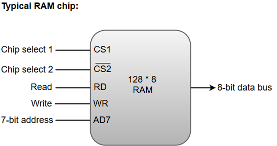
- A 128 * 8 RAM chip has a memory capacity of 128 words of eight bits (one byte) per word. This requires a 7-bit address and an 8-bit bidirectional data bus.
- The 8-bit bidirectional data bus allows the transfer of data either from memory to CPU during a read operation or from CPU to memory during a write operation.
- The read and write inputs specify the memory operation, and the two chip select (CS) control inputs are for enabling the chip only when the microprocessor selects it.
- The bidirectional data bus is constructed using three-state buffers.
- The output generated by three-state buffers can be placed in one of the three possible states which include a signal equivalent to logic 1, a signal equal to logic 0, or a high-impedance state.
Note: The logic 1 and 0 are standard digital signals whereas the high-impedance state behaves like an open circuit, which means that the output does not carry a signal and has no logic significance.
The following function table specifies the operations of a 128 * 8 RAM chip.
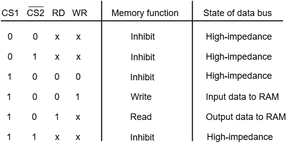
From the functional table, we can conclude that the unit is in operation only when CS1 = 1 and CS2 = 0. The bar on top of the second select variable indicates that this input is enabled when it is equal to 0.
ROM integrated circuit
The primary component of the main memory is RAM integrated circuit chips, but a portion of memory may be constructed with ROM chips.
A ROM memory is used for keeping programs and data that are permanently resident in the computer.
Apart from the permanent storage of data, the ROM portion of main memory is needed for storing an initial program called a bootstrap loader. The primary function of the bootstrap loader program is to start the computer software operating when power is turned on.
ROM chips are also available in a variety of sizes and are also used as per the system requirement. The following block diagram demonstrates the chip interconnection in a 512 * 8 ROM chip.
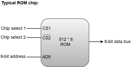
- A ROM chip has a similar organization as a RAM chip. However, a ROM can only perform read operation; the data bus can only operate in an output mode.
- The 9-bit address lines in the ROM chip specify any one of the 512 bytes stored in it.
- The value for chip select 1 and chip select 2 must be 1 and 0 for the unit to operate. Otherwise, the data bus is said to be in a high-impedance state.