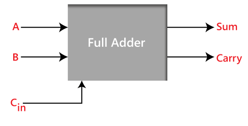
Full Adder
The half adder is used to add only two numbers. To overcome this problem, the full adder was developed. The full adder is used to add three 1-bit binary numbers A, B, and carry C. The full adder has three input states and two output states i.e., sum and carry.
Block diagram
Truth Table
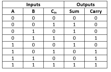
In the above table,
- ‘A’ and’ B’ are the input variables. These variables represent the two significant bits which are going to be added
- ‘Cin‘ is the third input which represents the carry. From the previous lower significant position, the carry bit is fetched.
- The ‘Sum’ and ‘Carry’ are the output variables that define the output values.
- The eight rows under the input variable designate all possible combinations of 0 and 1 that can occur in these variables.
Note: We can simplify each of the output ‘Boolean function’ with the help of the unique map method.
The SOP form can be obtained with the help of K-map as:
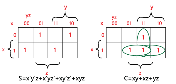
Sum = x’ y’ z+x’ yz+xy’ z’+xyz
Carry = xy+xz+yz
Construction of Half Adder Circuit:
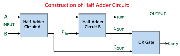
The above block diagram describes the construction of the Full adder circuit. In the above circuit, there are two half adder circuits that are combined using the OR gate. The first half adder has two single-bit binary inputs A and B. As we know that, the half adder produces two outputs, i.e., Sum and Carry. The ‘Sum’ output of the first adder will be the first input of the second half adder, and the ‘Carry’ output of the first adder will be the second input of the second half adder. The second half adder will again provide ‘Sum’ and ‘Carry’. The final outcome of the Full adder circuit is the ‘Sum’ bit. In order to find the final output of the ‘Carry’, we provide the ‘Carry’ output of the first and the second adder into the OR gate. The outcome of the OR gate will be the final carry out of the full adder circuit.
The MSB is represented by the final ‘Carry’ bit.
The full adder logic circuit can be constructed using the ‘AND’ and the ‘XOR’ gate with an OR gate.
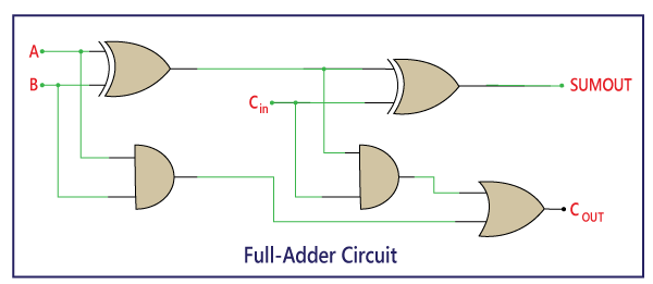
The actual logic circuit of the full adder is shown in the above diagram. The full adder circuit construction can also be represented in a Boolean expression.
Sum:
- Perform the XOR operation of input A and B.
- Perform the XOR operation of the outcome with carry. So, the sum is (A XOR B) XOR Cin which is also represented as:
(A ⊕ B) ⊕ Cin
Carry:
- Perform the ‘AND’ operation of input A and B.
- Perform the ‘XOR’ operation of input A and B.
- Perform the ‘OR’ operations of both the outputs that come from the previous two steps. So the ‘Carry’ can be represented as:
A.B + (A ⊕ B)