Integrated Circuits
An integrated circuit (IC) is manufactured using silicon material and mounted in a ceramic or plastic container (known as Chip). The basic components of an IC consist of electronic circuits for the digital gates. The various gates are interconnected inside an IC to form the required circuit.
The following categories can broadly classify an Integrated Circuit (IC):
SSI (Small Scale Integration Devices)
These type of devices contain several independent gates in a single package. The inputs and outputs of these gates are connected directly to the pins in the package. The number of logic gates are usually less than 10 and are limited by the number of pins available in the IC.
MSI (Medium Scale Integration Devices)
These type of devices has a complexity of approximately 10 to 200 gates in a single package. The basic components include decoders, adders, and registers.
LSI (Large Scale Integration Devices)
LSI devices contain about 200 to a few thousand gates in a single package. The basic components of an LSI device include digital systems, such as processors, memory chips, and programmable modules.
VLSI (Very Large Scale Integration Device)
This type of devices contains thousands of gates within a single package. The most common example of a VLSI device is a complex microcomputer chip.
Digital integrated circuits are also classified by their specific circuit technology to which they belong. The circuit technology is often referred to as Digital Logic Family. Each technology has its own basic electronic circuit and functions to perform.
The most common component in each technology is either a NAND, a NOR, or an inverter gate.
The most popular among the digital logic families include:
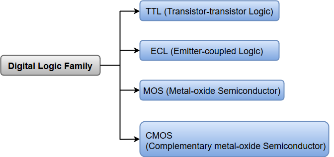
- TTL (Transistor-transistor Logic)
- ECL (Emitter-coupled logic)
- MOS (Metal-oxide semiconductor)
- CMOS (Complementary metal-oxide-semiconductor)
TTL (Transistor-transistor Logic)
The TTL technology was an upgraded version of a previous technology called as DTL (Diode-Transistor Logic). The DTL technology used to have diodes and transistors for the basic NAND gate. TTL came in existence when these diodes are replaced with transistors to improve the circuit operation.
There are several variations of the TTL like high-speed TTL, low-power TTL, Schottky TTL, low-power Schottky TTL, and advanced Schottky TTL.
The following circuit diagram shows a Standard TTL circuit and its configuration.
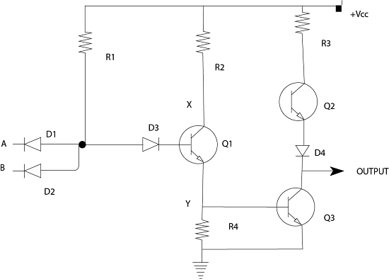
Features of TTL Family:
- The overall power supply voltage for TTL circuit is 5 volts, and the two logic levels are approximately 0 and 3.5 volts.
- A TTL circuit can support at most 10 gates at its output.
- The average propagation delay for a TTL circuit is about 9ns.
TTL Applications
- TTL is used as a switching device in driving lamps and relays.
- TTL is used in controller application for providing 0 to 5Vs.
- TTL families are mostly used in processors of minicomputers like DEC VAX.
- It is also used in printers and video display terminals.
ECL (Emitter-coupled Logic)
The ECL technology provides the highest-speed digital circuits in integrated form. An ECL circuit is used in supercomputers and signal processors where high speed is essential.
The transistors in ECL gates operate in a non-saturated state, a condition that allows the achievement of propagation delays of 1 to 2 nanoseconds.
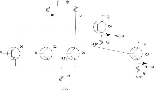
Features of ECL Family
- The logic gates continuously draw current even in the inactive state. Hence power consumption is more as compared to other logic families.
- ECL uses bipolar transistor logic where the transistors are not operated in the saturation region.
- The average propagation delay for an ECL gate is about 0.5 to 2ns.
MOS (Metal-oxide semiconductor)
The MOS (Metal-oxide semiconductor) is a unipolar transistor that depends on the flow of only one type of carrier, which may be electrons (n-channel) or holes (p-channel).
MOS technology is generally categorized in two basic forms:
- A p-channel MOS is referred to as PMOS.
- An n-channel MOS is referred to as NMOS.
PMOS
The operations performed by a PMOS logic family can be explained by considering a PMOS NAND gate.
The following circuit diagram shows a two input PMOS NAND gate.
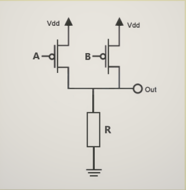
When a low logic is applied to either A or B, the transistor gets activated. This makes a connection between power supply and the output terminal.
When a low logic is applied, the output is raised to a logic high value. Otherwise, it will remain at logic low in other cases.
The pull-down resistor ‘R’ maintains the low logic unless a low logic is applied to either A or B.
NMOS
The structure of NMOS logic is similar to that of PMOS. However, instead of using PMOS transistors, here we will use NMOS transistors along with a pull-up resistor R.
The following circuit diagram shows a two input NMOS NAND gate.
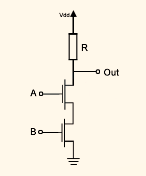
As shown in the circuit diagram, an NMOS NAND gate has two NMOS transistors connected in series from the output to the ground terminal.
A pull-up resistor is connected from the output terminal to the power supply.
When a high logic is applied to both inputs, both of the transistors get activated. This makes a connection between the output terminal and ground.
In case, any one of the input is at logic high, and the other one is at logic low, the transistor gets deactivated. This terminates the path between the output terminal and ground.
CMOS (Complementary metal-oxide semiconductor)
The complementary MOS or CMOS technology uses PMOS and NMOS transistors connected in a complementary manner in all circuits.
CMOS logic families are highly preferred in large-scale integrated circuits because of its high noise immunity and low power dissipation.
The following circuit diagram shows a Standard CMOS circuit and its configuration.
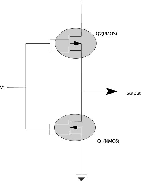
Q1 and Q2 are the respective NMOS and PMOS transistors connected in a complementary fashion.