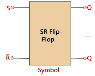
SR Flip Flop
The SR flip flop is a 1-bit memory bistable device having two inputs, i.e., SET and RESET. The SET input ‘S’ set the device or produce the output 1, and the RESET input ‘R’ reset the device or produce the output 0. The SET and RESET inputs are labeled as S and R, respectively.
The SR flip flop stands for “Set-Reset” flip flop. The reset input is used to get back the flip flop to its original state from the current state with an output ‘Q’. This output depends on the set and reset conditions, which is either at the logic level “0” or “1”.
The NAND gate SR flip flop is a basic flip flop which provides feedback from both of its outputs back to its opposing input. This circuit is used to store the single data bit in the memory circuit. So, the SR flip flop has a total of three inputs, i.e., ‘S’ and ‘R’, and current output ‘Q’. This output ‘Q’ is related to the current history or state. The term “flip-flop” relates to the actual operation of the device, as it can be “flipped” to a logic set state or “flopped” back to the opposing logic reset state.
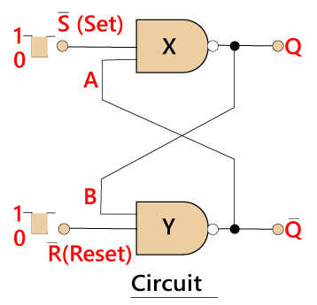
The NAND Gate SR Flip-Flop
We can implement the set-reset flip flop by connecting two cross-coupled 2-input NAND gates together. In the SR flip flop circuit, from each output to one of the other NAND gate inputs, feedback is connected. So, the device has two inputs, i.e., Set ‘S’ and Reset ‘R’ with two outputs Q and Q’ respectively. Below are the block diagram and circuit diagram of the S-R flip flop.
Block Diagram:
Circuit Diagram:
The Set State
In the above diagram, when the input R is set to false or 0 and the input S is set to true or 1, the NAND gate Y has an input 0, which will produce the output Q’ 1. The value of Q’ is faded to the NAND gate ‘X’ as input ‘A’, and now both the inputs of the NAND gate ‘X’ are 1(S=A=1), which will produce the output ‘Q’ 0.
Now, if the input R is changed to 1 with ‘S’ remaining 1, the inputs of NAND gate ‘Y’ is R=1 and B=0. Here, one of the inputs is also 0, so the output of Q’ is 1. So, the flip flop circuit is set or latched with Q=0 and Q’=1.
Reset State
The output Q’ is 0, and output Q is 1 in the second stable state. It is given by R =1 and S = 0. One of the inputs of NAND gate ‘X’ is 0, and its output Q is 1. Output Q is faded to NAND gate Y as input B. So, both the inputs to NAND gate Y are set to 1, therefore, Q’ = 0.
Now, if the input S is changed to 0 with ‘R’ remaining 1, the output Q’ will be 0 and there is no change in state. So, the reset state of the flip flop circuit has been latched, and the set/reset actions are defined in the following truth table:
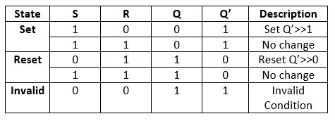
From the above truth table, we can see that when set ‘S’ and reset ‘R’ inputs are set to 1, the outputs Q and Q’ will be either 1 or 0. These outputs depend on the input state S or R before the input condition exist. So, when the inputs are 1, the states of the outputs remain unchanged.
The condition in which both the inputs states are set to 0 is treated as invalid and must be avoided.