Timing Diagram of MOV Instruction
In order to understand the timing diagram of MOV instruction, we have to first learn about the MOV instruction.
MOV Instruction:
The MOV instruction is used to copy the data of item, which is referred to as the second operand of the instruction (Constant value, register content, or memory content), into the location, which is referred to by its first operand (memory or register). In the MOV instruction, it is not possible to do direct memory to memory moves, but it is possible to do register to register moves. If there is some case in which memory transfers are desired, then the content of source memory will be first loaded into a register. After that, it can be stored in a destination memory address.
Syntax: The syntax of MOV instruction is described as follows:
Problem: Here, we have an instruction given below, and we have to draw the timing diagram of that instruction.
The above instruction is used to copy the content of first register into the second register without changing the content of first or source register.
Example:
Here B is used to indicate the destination register, and C is used to indicate the source register. In the above example, the content of C needs to be transferred into B.
Algorithm:
The above instruction MOV B, C only requires 1 byte. So we only require one memory address to store the instruction completely. For example:
The above instruction needs the opcode fetching. So we can generate the timing diagram with the help of 4T states. For the opcode fetch, the IO/M (low active) = 0, S0 = 1, and S1 = 1.
Now we will draw the timing diagram of MOV instruction, which is described as follows:
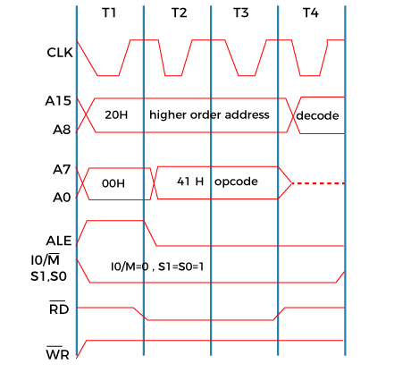
In Opcode fetch (t1-t4 states):
00: It is used to indicate the lower bit of address in which opcode is stored.
20: It is used to indicate the higher bit of address in which opcode is stored.
ALE: It is used to send signals for data buses and multiplexed addresses. Only in t1, it will be used to fetch the lower bit of address with the help of address bus. In all the other cases, it will be used as a data bus.
RD (Low active): In t1 and t4, the signal is 1, which shows that none of the data is ready by a microprocessor. In t2 and t3, the signal is 0, which shows that the data is ready by a microprocessor.
WR (Low active): Here, the signal is 1 throughput which shows that none of the data is written with the help of a microprocessor.
IO/M (Low active): Here, the signal is 1 throughput which shows that the operation is performing on memory.
S0 and S1: If S0 and S1 try to fetch the opcode, then they will be 1.