Verilog Gate Delay
Verilog gate delays specify how values propagate through nets or gates. The gate delay declaration specifies a time needed to propagate a signal change from the gate input to its output.
The gate delay declaration can be used in gate instantiations. The delays can also be used for delay control in procedural statements.
Digital elements are binary entities and only hold either of the two values, 0 and 1. The transition from 0 to 1 and 1 to 0 has a transitional delay, and therefor each gate element propagates the value from input to its output.
For example, a two-input AND gate has to switch the output to 1 if both inputs become 1 and back to 0 when inputs become 0.
The net delay declaration specifies a time needed to propagate values from drivers through the net. It can be used in continuous assignments and net declarations.
This gate and pin to pin delays can be specified in Verilog when instantiating logic primitives.
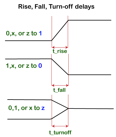
Rise, Fall, and Turn-Off Delays
The delays declaration can contain up to three values, such as rise, fall, and turn-off delays.
- The time taken for the output of a gate to change from some value to 1 is called a rise delay.
- The time taken for the output of a gate to change form some value to 0 is called a fall delay.
- The time taken for the output of a gate to change from some value to high impedance is called turn-off delay.
If only one delay value is specified, then it is used for all signal changes. The default delay is zero.
If two delays are specified, then the first delay specifies the rise delay, and the second delay specifies the fall delay.
If the signal changes to high-impedance or unknown, then the smaller value will be used.
If three values are given, then the first value specifies the rise delay, the second specifies the fall delay, and the third specifies the turn-off delay. If the signal changes to an unknown value, then the smallest of these three values will be used.
These delays apply to any signal as they all can rise or fall anytime in real circuits and are not restricted to only outputs of gates. There are three ways to represent gate delays.
- One delay format
- Two delay format
- Three delay format
The two delay format can be applied to most primitives whose outputs do not transition to high impedance.
A three delay format cannot be applied to an AND gate because the output will not go to Z for any input combination.
If only a single delay is specified, all three types of delays will use the same given value.
If there are two delays specified, the first one represents the rise, and the second one represents the fall delay.
If there are three delays specified, they represent rise, fall, and turn-off delays, respectively.
1. One Delay Format
Now, See that the output of AND gates change 2 time units after one of its inputs change.
For example, b becomes 1 while a is already 1 at T=20. But the output becomes 1 only at T=22. Similarly, a goes back to zero at T=30, and the output gets the new value at T=32.
Gate delay is specified as 3-time units for BUFIF0. If b changes from 0 to 1 while a is already at 1, then the output takes 3-time units to get updated to Z and finally does so at T=23.
Output
ncsim> run T=0 a=0 b=0 and=x bufif0=x T=2 a=0 b=0 and=0 bufif0=x T=3 a=0 b=0 and=0 bufif0=0 T=10 a=1 b=0 and=0 bufif0=0 T=13 a=1 b=0 and=0 bufif0=1 T=20 a=1 b=1 and=0 bufif0=1 T=22 a=1 b=1 and=1 bufif0=1 T=23 a=1 b=1 and=1 bufif0=z T=30 a=0 b=1 and=1 bufif0=z T=32 a=0 b=1 and=0 bufif0=z T=40 a=0 b=0 and=0 bufif0=z T=43 a=0 b=0 and=0 bufif0=0 ncsim: *W,RNQUIE: Simulation is complete.
2. Two Delay Format
Let’s apply the same testbench shown above to a different Verilog model shown below where rise and fall delays are explicitly mentioned.
And it produces the following output, such as:
3. Three Delay Format
The three delay format code gives the following output:
Min, Typ, and Max Delays
Delays are neither the same in different parts of the fabricated chip nor the same for different temperatures and other variations. So Verilog also provides an extra level of control for each of the delay types mentioned above.
Every digital gate and transistor cell has a minimum, typical, and maximum delay specified based on process node and is typically provided by libraries from fabrication foundry.
For rise, fall, and turn-off delays, the three values min, typ, and max can be specified and stand for minimum, typical and maximum delays.
This is another level of delay control in Verilog. Only one of the min, typ, and max values can be used in the entire simulation run.
It is specified at the start of the simulation and depends on the simulator used. The typ is the default value.
The min value is the minimum delay value that the gate is expected to have.
The typ value is the typical delay value that the gate is expected to have.
The max value is the maximum delay value that the gate is expected to have.
The output looks like: