What is Interleaved Memory?
Interleaved memory is designed to compensate for the relatively slow speed of dynamic random-access memory (DRAM) or core memory by spreading memory addresses evenly across memory banks. In this way, contiguous memory reads and writes use each memory bank, resulting in higher memory throughput due to reduced waiting for memory banks to become ready for the operations.
It is different from multi-channel memory architectures, primarily as interleaved memory does not add more channels between the main memory and the memory controller. However, channel interleaving is also possible, for example, in Freescale i.MX6 processors, which allow interleaving to be done between two channels. With interleaved memory, memory addresses are allocated to each memory bank.
Example of Interleaved Memory
It is an abstraction technique that divides memory into many modules such that successive words in the address space are placed in different modules.
Suppose we have 4 memory banks, each containing 256 bytes, and then the Block Oriented scheme (no interleaving) will assign virtual addresses 0 to 255 to the first bank and 256 to 511 to the second bank. But in Interleaved memory, virtual address 0 will be with the first bank, 1 with the second memory bank, 2 with the third bank and 3 with the fourth, and then 4 with the first memory bank again.
Hence, the CPU can access alternate sections immediately without waiting for memory to be cached. There are multiple memory banks that take turns for the supply of data.
In the above example of 4 memory banks, data with virtual addresses 0, 1, 2 and 3 can be accessed simultaneously as they reside in separate memory banks. Hence we do not have to wait to complete a data fetch to begin the next operation.
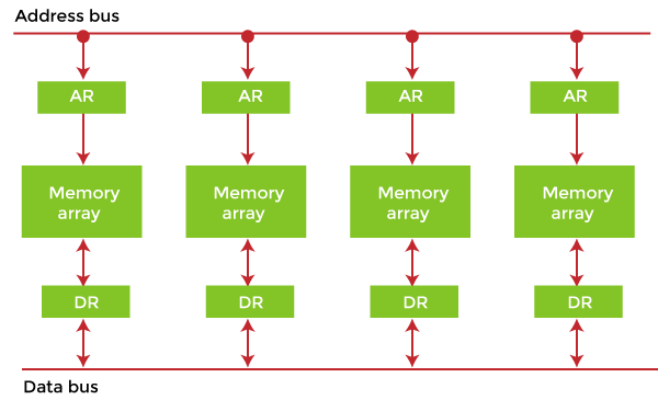
An interleaved memory with n banks is said to be n-way interleaved. There are still two banks of DRAM in an interleaved memory system, but logically, the system seems one bank of memory that is twice as large.
In the interleaved bank representation below with 2 memory banks, the first long word of bank 0 is flowed by that of bank 1, followed by the second long word of bank 0, followed by the second long word of bank 1 and so on.
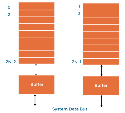
The following image shows the organization of two physical banks of n long words. All even long words of the logical bank are located in physical bank 0, and all odd long words are located in physical bank 1.
Why do we use Memory Interleaving?
When the processor requests data from the main memory, a block (chunk) of data is transferred to the cache and then to processor. So whenever a cache miss occurs, the data is to be fetched from the main memory. But main memory is relatively slower than the cache. So to improve the access time of the main memory, interleaving is used.
For example, we can access all four modules at the same time, thus achieving parallelism. The data can be acquired from the module using the higher bits. This method uses memory effectively.
Types of Interleaved Memory
In an operating system, there are two types of interleaved memory, such as:
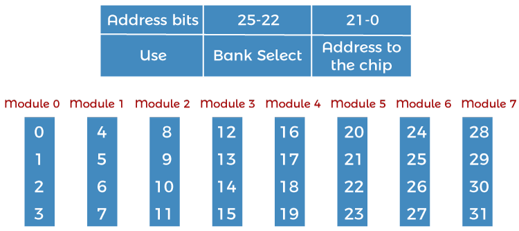
1. High order interleaving: In high order memory interleaving, the most significant bits of the memory address decides memory banks where a particular location resides. But, in low order interleaving the least significant bits of the memory address decides the memory banks.
The least significant bits are sent as addresses to each chip. One problem is that consecutive addresses tend to be in the same chip. The maximum rate of data transfer is limited by the memory cycle time. It is also known as Memory Banking.
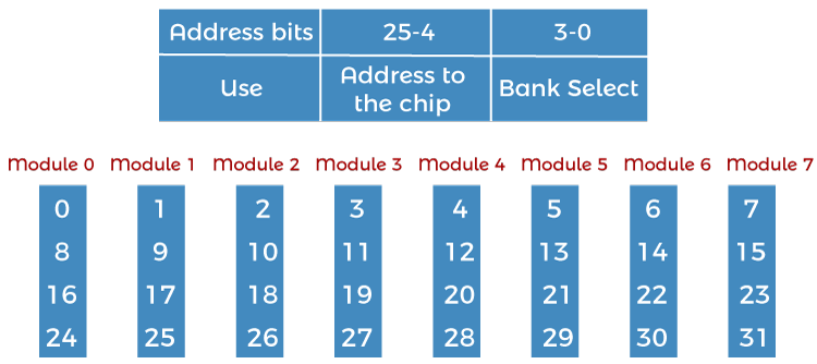
2. Low order interleaving: The least significant bits select the memory bank (module) in low-order interleaving. In this, consecutive memory addresses are in different memory modules, allowing memory access faster than the cycle time.
Benefits of Interleaved Memory
An instruction pipeline may require instruction and operands both at the same time from main memory, which is not possible in the traditional method of memory access. Similarly, an arithmetic pipeline requires two operands to be fetched simultaneously from the main memory. So, to overcome this problem, memory interleaving comes to resolve this.
- It allows simultaneous access to different modules of memory. The modular memory technique allows the CPU to initiate memory access with one module while others are busy with the CPU in reading or write operations. So, we can say interleave memory honors every memory request independent of the state of the other modules.
- So, for this obvious reason, interleave memory makes a system more responsive and fast than non-interleaving. Additionally, with simultaneous memory access, the CPU processing time also decreases and increasing throughput. Interleave memory is useful in the system with pipelining and vector processing.
- In an interleaved memory, consecutive memory addresses are spread across different memory modules. Say, in a byte-addressable 4 way interleave memory, if byte 0 is in the first module, then byte 1 will be in the 2nd module, byte 2 will be in the 3rd module, byte 3 will be in the 4th module, and again byte 4 will fall in the first module, and this goes on.
- An n-way interleaved memory where main memory is divided into n-banks and system can access n operands/instruction simultaneously from n different memory banks. This kind of memory access can reduce the memory access time by a factor close to the number of memory banks. In this memory interleaving memory location, i can be found in bank i mod n.
Interleaving DRAM
Main memory is usually composed of a collection of DRAM memory chips, where many chips can be grouped together to form a memory bank. With a memory controller that supports interleaving, it is then possible to layout these memory banks so that the memory banks will be interleaved.
Data in DRAM is stored in units of pages. Each DRAM bank has a row buffer that serves as a cache for accessing any page in the bank. Before a page in the DRAM bank is read, it is first loaded into the row-buffer. If the page is immediately read from the row-buffer, it has the shortest memory access latency in one memory cycle. Suppose it is a row buffer miss, which is also called a row-buffer conflict. It is slower because the new page has to be loaded into the row-buffer before it is read. Row-buffer misses happening as access requests on different memory pages in the same bank are serviced. A row-buffer conflict incurs a substantial delay for memory access. In contrast, memory accesses to different banks can proceed in parallel with high throughput.
In traditional layouts, memory banks can be allocated a contiguous block of memory addresses, which is very simple for the memory controller and gives an equal performance in completely random access scenarios compared to performance levels achieved through interleaving. However, memory reads are rarely random due to the locality of reference, and optimizing for close together access gives far better performance in interleaved layouts.
The way memory is addressed does not affect the access time for memory locations that are already cached, impacting only on memory locations that need to be retrieved from DRAM.