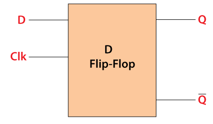
D Flip Flop
In SR NAND Gate Bistable circuit, the undefined input condition of SET = “0” and RESET = “0” is forbidden. It is the drawback of the SR flip flop. This state:
- Override the feedback latching action.
- Force both outputs to be 1.
- Lose the control by the input, which first goes to 1, and the other input remains “0” by which the resulting state of the latch is controlled.
We need an inverter to prevent this from happening. We connect the inverter between the Set and Reset inputs for producing another type of flip flop circuit called D flip flop, Delay flip flop, D-type Bistable, D-type flip flop.
The D flip flop is the most important flip flop from other clocked types. It ensures that at the same time, both the inputs, i.e., S and R, are never equal to 1. The Delay flip-flop is designed using a gated SR flip-flop with an inverter connected between the inputs allowing for a single input D(Data).
This single data input, which is labeled as “D” used in place of the “Set” input and for the complementary “Reset” input, the inverter is used. Thus, the level-sensitive D-type or D flip flop is constructed from a level-sensitive SR flip flop.
So, here S=D and R= ~D(complement of D)
Block Diagram
Circuit Diagram
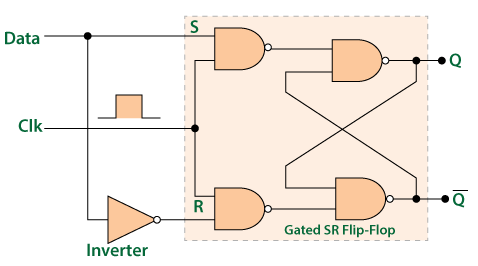
We know that the SR flip-flop requires two inputs, i.e., one to “SET” the output and another to “RESET” the output. By using an inverter, we can set and reset the outputs with only one input as now the two input signals complement each other. In SR flip flop, when both the inputs are 0, that state is no longer possible. It is an ambiguity that is removed by the complement in D-flip flop.
In D flip flop, the single input “D” is referred to as the “Data” input. When the data input is set to 1, the flip flop would be set, and when it is set to 0, the flip flop would change and become reset. However, this would be pointless since the output of the flip flop would always change on every pulse applied to this data input.
The “CLOCK” or “ENABLE” input is used to avoid this for isolating the data input from the flip flop’s latching circuitry. When the clock input is set to true, the D input condition is only copied to the output Q. This forms the basis of another sequential device referred to as D Flip Flop.
When the clock input is set to 1, the “set” and “reset” inputs of the flip-flop are both set to 1. So it will not change the state and store the data present on its output before the clock transition occurred. In simple words, the output is “latched” at either 0 or 1.
Truth Table for the D-type Flip Flop
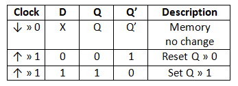
Symbols ↓ and ↑ indicates the direction of the clock pulse. D-type flip flop assumed these symbols as edge-triggers.